
Google's 8th Generation TPU Diversifies: Separating TPU 8t for Training and TPU 8i for Inference
Google has designed its 8th generation TPU into two distinct versions, TPU 8t for training and TPU 8i for inference and reinforcement learning, to address different workload bottlenecks. Meanwhile, NVIDIA is countering the trend of big tech companies developing in-house chips by offering interconnect and memory technologies like NVLink Fusion and NVHBM.
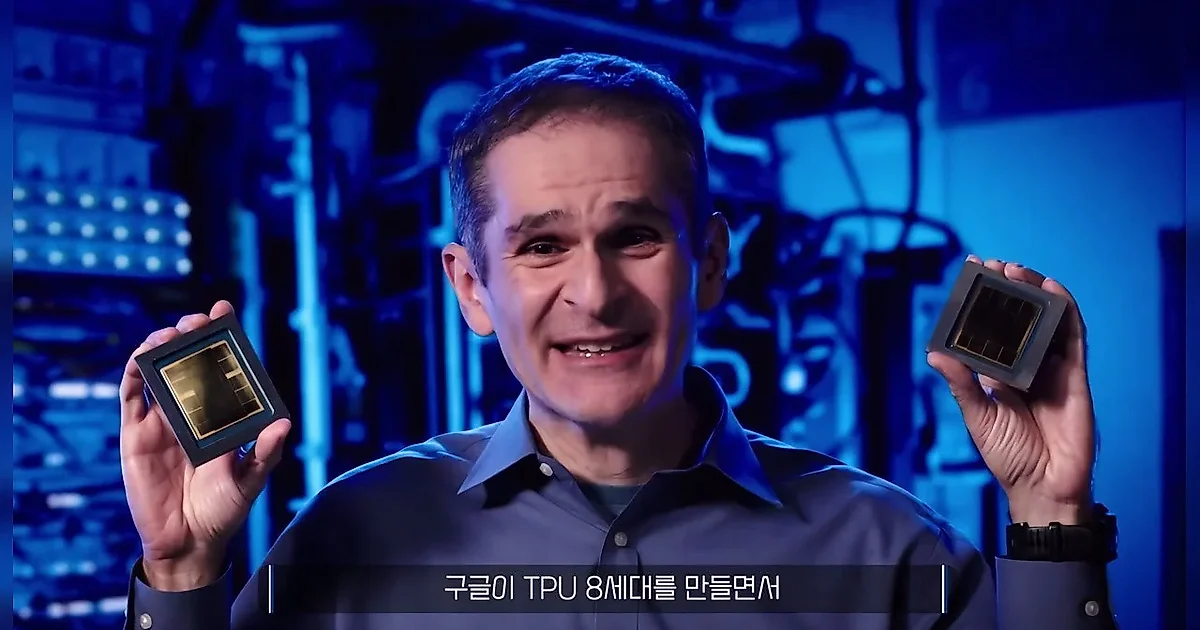
As big tech companies accelerate the development of their own AI chips (xPU), chip design purposes are being subdivided according to specific workloads. Google recently revealed that its 8th generation TPU has been designed as a dual system, consisting of 'TPU 8t' for training and 'TPU 8i' for inference and reinforcement learning. This decision stems from the judgment that the bottlenecks occurring during the training and inference stages are different.
Training-focused 8t and Inference-focused 8i: Differences in chip design according to workload
According to the video, the TPU 8t, which aims for large-scale training, is optimized to process thousands of chips as a single large computational unit. In the training process, the key is to ensure that thousands of chips continue calculating without rest, rather than focusing on the response speed of individual chips. To achieve this, the TPU 8t includes Sparse Core, which handles the task of irregularly reading massive embedding tables, and possesses a scale that can connect up to 9,600 chips in a single superpod.
On the other hand, the TPU 8i, tailored for the inference stage that generates answers for users, focused on data processing efficiency. During inference, the use of KV cache to store previous information and data movement during the token generation process are crucial. Accordingly, the TPU 8i has increased its internal fast memory, SDRAM, capacity up to 384MB and is equipped with CAE, a communication device that quickly gathers calculation results from multiple chips. In particular, it uses the Board Fly connection method to reduce data movement time in MoE (Mixture of Experts) models.
Limitations of in-house chips, the versatility of GPUs, and the software ecosystem
In-house chips have the advantage of being able to be designed by knowing the exact calculation patterns of specific models. Google creates chips reflecting the calculation methods of Gemini, while Meta creates chips reflecting the operation patterns of its own recommendation and advertising models. However, since it takes a long time from chip design to data center deployment, there is a risk that dedicated circuits could become useless if a new AI model structure emerges. In contrast, NVIDIA GPUs possess the versatility to respond quickly to new calculation methods through software and library updates.
The software ecosystem is also a critical variable. NVIDIA has established an environment where developers can easily migrate existing code through CUDA. To complement this, Google operates XLA, a compiler that converts model code into a chip execution form. XLA plays a role in increasing the utility of TPUs by improving memory access efficiency through Fusion technology, which bundles different calculations into one.
NVIDIA's response strategy: NVLink Fusion and NVHBM
In response to the trend of big tech companies shifting to in-house chips, NVIDIA is adopting a strategy to ensure that even if customers create their own chips, they use NVIDIA's interconnect and memory technologies. A representative technology is NVLink Fusion. This allows not only NVIDIA GPUs but also xPUs or CPUs directly made by customers to be integrated into NVIDIA's interconnect network. In fact, Amazon (AWS) is currently conducting cooperation to connect its in-house chip, Trainium, with NVIDIA's NVLink technology.
Furthermore, NVIDIA has proposed a way to enhance the performance of in-house chips through NVHBM technology. This method moves the functions of HBM toward the base die, helping customers allocate more space to calculation circuits when designing their own chips. NVIDIA explained that through this technology, they can secure up to 25% of the computation die area and increase memory bandwidth by 30%. This is interpreted as a strategy to ensure that even if customers manufacture the computation chips themselves, they maintain NVIDIA's technology for the connections and memory infrastructure surrounding the chips.



0Comments
Comments are currently disabled.