
Silicon photonics and CPO technology to address AI data bottlenecks
Silicon photonics and Co-Packaged Optics (CPO) are emerging as critical technologies to overcome data transmission limits in AI data centers by replacing electrical signals with light.
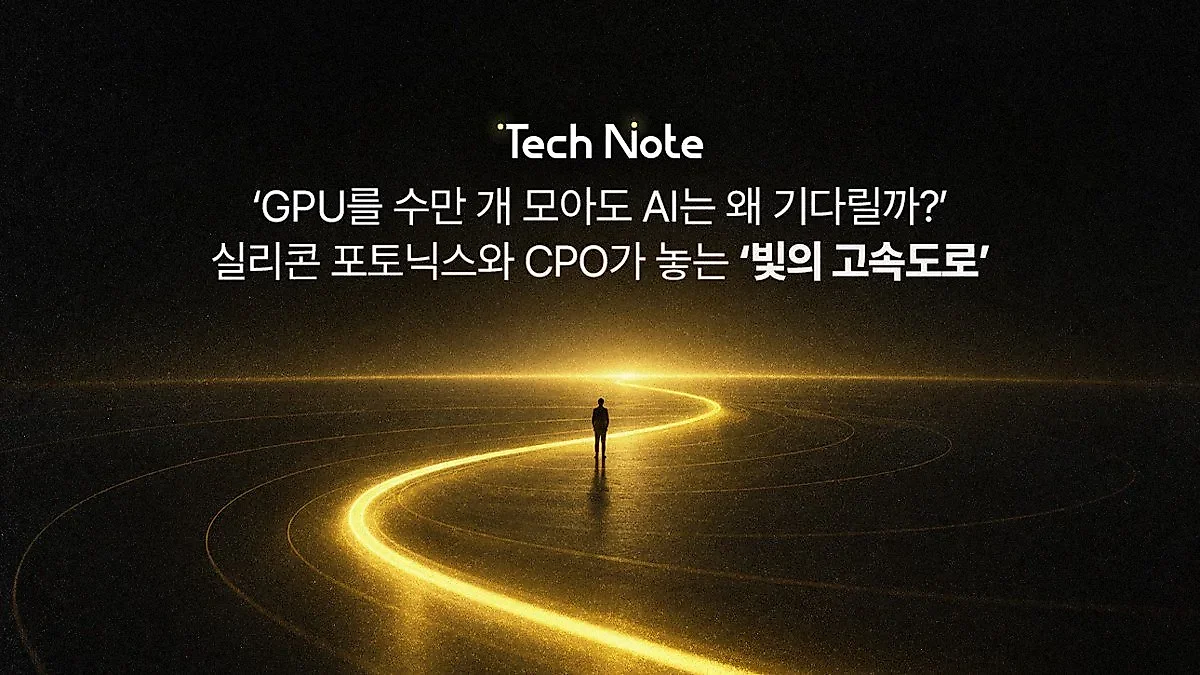
Silicon photonics and Co-Packaged Optics (CPO) are emerging as vital technologies to overcome data bottlenecks in AI factories, where Meta confirmed that CPO switch systems could reduce optical connection power consumption by approximately 65% compared to existing pluggable methods.
In the era of AI, competitiveness depends more on the efficiency of data movement than on the computational speed of individual GPUs (Graphics Processing Units). Even with the fastest computing chips, the entire system falls into a waiting state if the pathways carrying the data are narrow. Recently, "Silicon Photonics"—which converts electrical signals into light—and "Co-Packaged Optics (CPO)" technology have gained attention as key variables determining the performance of AI data centers, also known as "AI factories."
Data Bottlenecks Hindering GPU Computing Speed
When training large-scale AI models, numerous GPUs share a single model and constantly exchange calculation results and data. While the computing power of the GPUs themselves is excellent, a bottleneck occurs if the pathways for retrieving data from memory or transferring data between GPUs are insufficient. This is similar to a situation where factories equipped with the latest facilities are clustered together, but the roads connecting them are too narrow to allow raw materials and finished products to move in a timely manner.
Until now, connections between semiconductors have relied primarily on electrical signals through "copper wiring." While copper is efficient over short distances, signal strength weakens as data transmission speeds increase and distances grow longer. Using devices like repeaters to restore weakened signals consumes additional power, which leads to massive heat generation and cooling burdens. As AI models grow larger, the power and heat issues of copper wiring become decisive obstacles hindering the scalability of AI factories.
Silicon Photonics and CPO: Creating Paths of Light on Chips
Silicon photonics emerged to overcome these limitations. This technology utilizes existing semiconductor manufacturing processes to implement "optical waveguides"—microscopic paths for light—on silicon chips. Through Wavelength Division Multiplexing (WDM) technology, multiple wavelengths of light can be carried on a single optical fiber, allowing for a dramatic increase in transmission capacity.
Since silicon is an unfavorable material for directly generating light, methods that receive light via an External Laser Source (ELS) are primarily used. Co-Packaged Optics (CPO) maximizes this technology. Previously, switch chips and optical modules were separate, requiring electrical signals to travel long distances across a substrate; however, CPO places the optical engine right next to the switch ASIC (Application-Specific Integrated Circuit). This method increases bandwidth density and reduces power consumption by minimizing the electrical sections where data moves and connecting longer sections with optical fibers.
In fact, Meta stated that its evaluation of a CPO switch system at the 2025 European Conference on Optical Communication (ECOC) confirmed that power consumption in the optical connection portion could be reduced by approximately 65% compared to existing pluggable methods. Global big tech companies, including NVIDIA and Broadcom, are also entering the commercialization race by introducing network products that apply this CPO technology.
Combining HBM and CPO Toward "Wait-Free AI"
While CPO resolves bottlenecks in network sections, HBM (High Bandwidth Memory) serves to supply data right next to the GPU. Even if HBM increases the data supply speed by being adjacent to the GPU, overall performance will not rise if communication (networking) between GPUs is blocked. Ultimately, the completion of an AI factory depends on the harmony between memory and network technologies.
In the future, "Memory Pooling" technology, which efficiently shares memory resources, and the CXL (Compute Express Link) standard that supports it, are highly likely to combine with silicon photonics. By expanding the paths to access the memory pool using light, it will be possible to use massive memory capacities flexibly while reducing the power burden.
Ultimately, the decisive factor for future AI semiconductors lies not in the performance of a single chip, but in packaging and optical technologies that bind GPUs, memory, and networks into one organic system. The most powerful AI factories are expected to be those that do not necessarily have the fastest GPUs, but those where numerous GPUs and memories work together organically without waiting for one another.
Source: news.skhynix.co.kr

0Comments
Comments are currently disabled.